When national security organisations use electronic equipment in sensitive environments, they must be sure every element has been properly assured.
In its latest challenge, HMGCC Co-Creation wants organisations to get involved in a five-month project, developing ways to robustly assure printed circuit boards (PCBs).
The innovative methods used need to image and verify the complete manufactured PCB stack-up, providing assurance they will function where and when they are most needed.
HMGCC Co-Creation will provide funding for time, material, overheads, and other indirect expenses.
The challenge
Context
All organisations associated with national security undertake sensitive and classified daily tasks, and there is the invariable need to use electronic equipment. Sensitive equipment may be sourced from a range of suppliers varying from bespoke construction by HMGCC to less well-established third-party routes. With all routes, there is a requirement to conduct due diligence on the constituent parts of an electronic system – ensuring functionality and security.
The focus of this challenge is to non-destructively image and verify printed circuit boards (PCB), specifically focusing on analysing copper traces through both the external and internal stack-up layers of complex multi-layer FR4 PCBs.
The gap
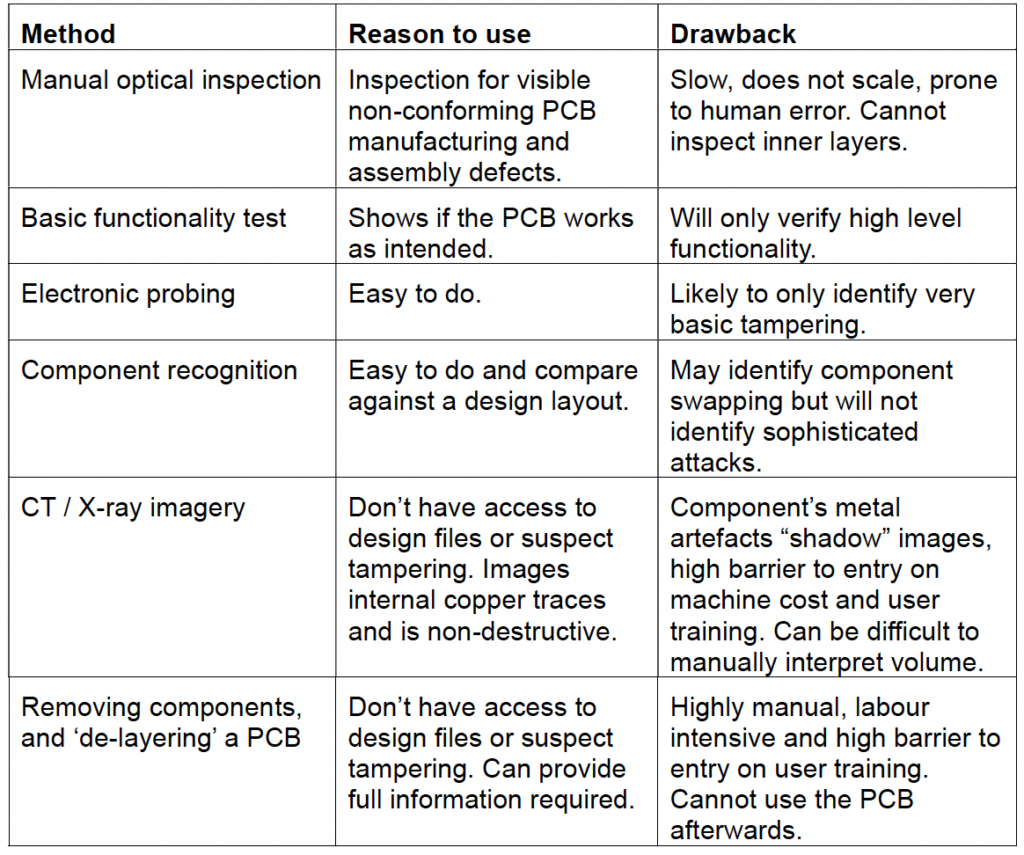
There exists capability to assure how a PCB functions and compare this to the intended design, or perhaps where there is no accessible design file. Displayed in table 1 is a non-exhaustive list of methods, the reason to use them and their drawbacks.
A PCB for verification could consist of multiple (potentially 10 or more) layers of copper traces, bonded on to FR4 glass epoxy substrates and laminated together. Each copper trace could be less than 35um in height, less than 100um in width and a copper clad layer less than 150um thick. On each PCB would be assembled a variety of electronic components of varying sizes and densities.
The variations in density and size of placed electronic components, thickness of the PCB, multiple copper trace layers and small feature sizes makes it very challenging to image copper traces on internal layers. Density variations will also likely cause shadowing across the imaged copper traces and whatever novel imaging method or technique is proposed, the capability to interpret this imperfect imagery to verify the copper trace routing and features is a requirement.
To scale PCB assurance capability on high value equipment that must be usable after examination, requires development of non-destructive and novel methods to image and interpret the images of copper traces throughout complex multilayer PCBs to quickly assure that only intended functionality and connections are present, while retaining a low barrier to entry of use for the analyst.

Example use case
A national security organisation is about to launch 10 new products in support of critical operational work. These products are portable, complex pieces of electronic equipment.
This equipment has been produced through collaboration including national security engineering specialists who have the full context of the project, trusted industrial partners who are aware of engineering requirements, and subcontracted third parties working on specific parts of the development. Thorough review of design and components helps provide appropriate assurance.
Kate, an assurance engineer, leads a team to review delivered hardware, testing each of the 10 products and every single item prior to their use by national security customers.
This used to be a mammoth task and not always possible with the complexity of multi-layer FR4 based PCBs. But, by using the newly developed non-destructive PCB verification machine, the team can cycle through each device rapidly. Added to this, it is easy to use and requires minimal training of staff.
Where a design file is present against which to compare the PCB images, the machine images the copper traces throughout the PCB stack-up and identifies the components to build a representative CAD/electronic design specification and compares this to the design file. The software also automatically flags if there are anomalies against the original design files, for further investigation.
In situations where a design file is not available, the machine uses artificial intelligence (AI) weightings to segment the individual images across the various FR4 layers to effectively ‘build’ a design file. The AI determines the probability of each image segment being from the same (or different) layer on the PCB, and groups these segments together to extract the copper trace routing on and between layers. This approach of probabilistically grouping the image segments so that they are provisionally assigned as belonging to a PCB layer helps with removing image artifacts in the AI-derived design file, such as the ‘shadowing’ sometimes seen from a CT scan.
Once each product has been analysed, Kate’s team can confirm the delivered hardware meets the same specification as the design file.
Project scope
Proposals should be focused on a proof of concept at Technology Readiness Level (TRL) 2-4, to be demonstrated towards the end of the six- month project, with a view to further development in future phases of work.
Desirable functions:
- Method can image copper traces throughout multi-layered FR4 based PCBs.
- Method works around possible shadowing or blocking effect from attached components.
- Machine vision and machine learning processes to interpret images.
- Direct and easy comparison of imaged PCB against original design files.
- Easy to use and minimal training required.
- Reasonably fast process (less than one day per PCB).
- Equipment must be useable within a normal lab setting, i.e. not be prohibitively large or hazardous.
What we don’t want:
- Horizon scanning
- Report of theoretical techniques
- Technology available more than 5 years from now
Key dates
15 July
Competition opens.
13 August
Deadline for questions.
20 August
Clarifying questions published.
29 August
Competition closes at 5pm.
09 September
Applicant notified.
17 September
Pitch day in Milton Keynes.
21 October
Target project kick-off.
Check back to this page for regular updates.
Eligibility
This challenge is open to sole innovators, industry, academic and research organisations of all types and sizes. There is no requirement for security clearances.
Solution providers or direct collaboration from countries listed by the UK government under trade sanctions and/or arms embargoes, are not eligible for HMGCC Co-Creation challenges.
DOCUMENTS AND LINKS
For further information including routes to apply, HMGCC Co-Creation terms and conditions and FAQs.